NEWS
l World market is dominated by two global manufacturers ... Market introduction as early as this year
l Construction of a semiconductor material cluster in Cheonan ... Increase in domestic portion of semiconductor materials to 48%
SKC is leading the effort to localize high-end blank mask products which are used as core materials for the semiconductor exposure process. A blank mask is a core material used to engrave electronic circuit patterns on a semiconductor wafer, and high-end blank masks have been dependent on imports.
SKC recently began producing prototypes for customer certification at its high-end blank mask factory in Cheonan, Chungnam. It invested about 43.0 billion won and began the construction of the factory in April last year, and completed the construction in December. Since the completion, they have been preparing for mass production. Its goal is to start commercialization as early as this year after the customer’s certification.
The factory is located in a site within SKC Hi-tech & Marketing’s Cheonan Factory. SKC decided to construct a semiconductor material cluster on its site. It plans to use the Cheonan cluster as a hub to increase the local portion, which currently is around 50%, of semiconductor materials.
A blank mask is a raw material of photomask that is used for engraving electronic circuit patterns on a semiconductor wafer. It is made by coating a _ meta_l film and a photosensitive film over quartz. A photomask is produced by forming a circuit pattern on it. Compared to photograph film, a blank mask is analogous to the film before shooting, and a photomask is analogous to the film after shooting. When light is emitted to a photomask placed on a semiconductor wafer, a chemical reaction occurs in the path of the emitted light to _ create_ a circuit.
The blank mask market has been growing every year. It is because the demands keep increasing as the semiconductor manufacturers are actively expanding the capacity, and its process increased as the process has become a nano level. According to SKC’s survey, the size of the world market is expected to grow by 7% each year from 800 billion won in 2018 to 1.3 trillion won in 2025.
Two Japanese global manufactures account for 95% of the market. In particular, they are known to account for more than 99% of the high-end market. It is because the entry barrier is high. Korea is also dependent on imports for most of the high-end blank masks needed for the manufacturing of semiconductors.
SKC decided to enter the market _ base_d on its technical knowledge accumulated over the years. To manufacture a blank master, a thin _ meta_l film and a thin photosensitive film on a nanometer level must be coated over quartz. The high-end models require thinner films coated in multiple _ layer_s uniformly. SKC has the necessary vacuum deposition technology and experience, as well as the knowledge for a super clean dust-free management.
“Having implemented the BM innovation for the past several years, SKC completed phase 1 and is currently implementing the phase 2 BM innovation which are centered on semiconductor, mobility, eco-friendly, and display businesses. The SKC semiconductor material cluster in Cheonan is part of our efforts to advance the semiconductor business and increase the localization,” an SKC official said. [End]
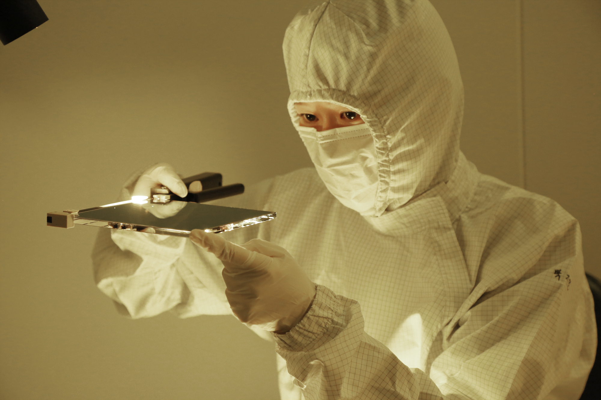
[An SKC employee is inspecting a prototype of the blank mask that is the core material for the semiconductor exposure process.]
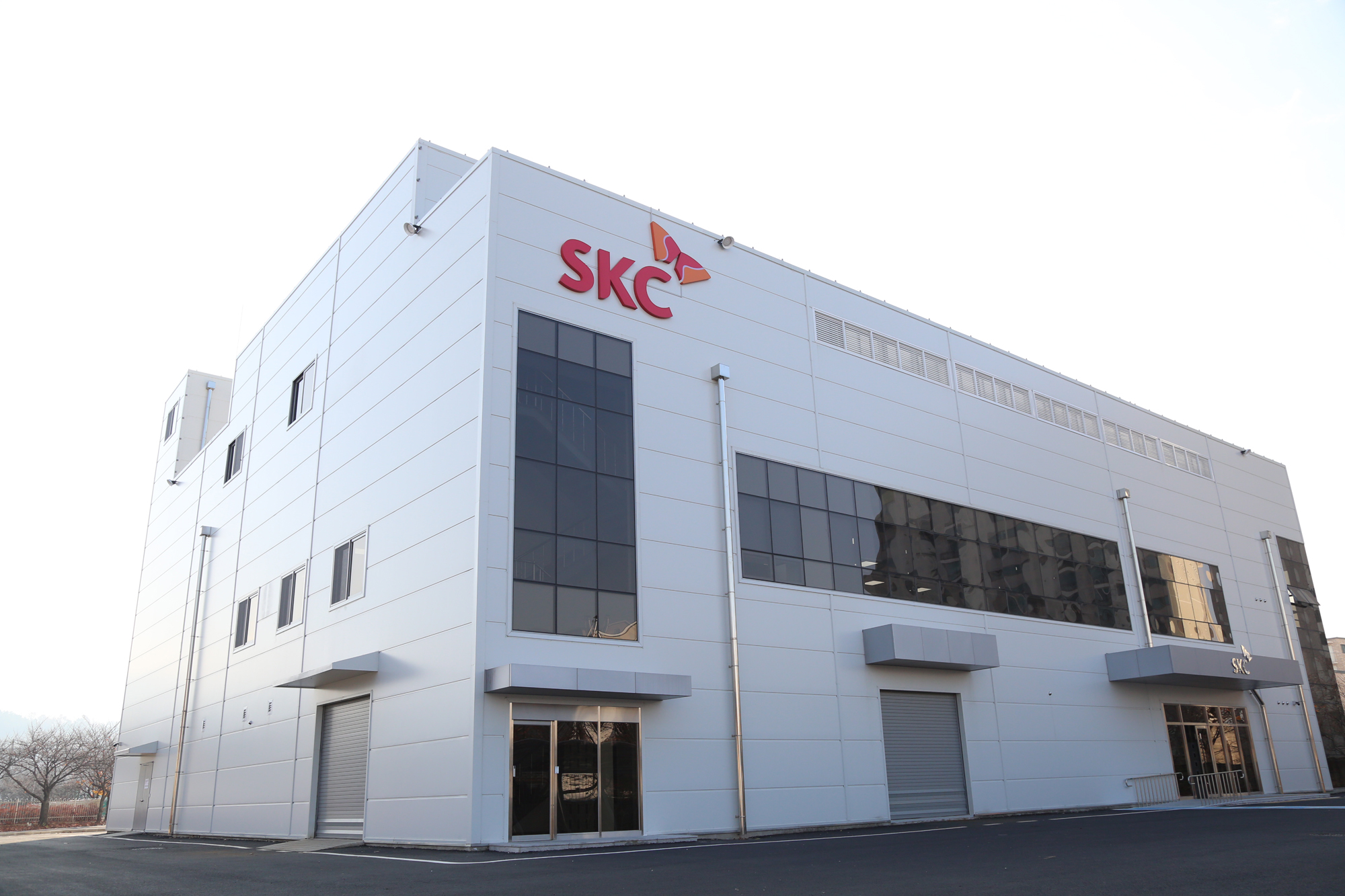
[View of the SKC blank mask factory constructed in SKC Hi-tech & Marketing’s Cheonan Factory. SKC plans to construct a semiconductor material cluster on the site.]
Copyright by SKC. All rights reserved.
